Top Stories
China’s Breakthrough Tech Reduces Microchip Defects by 99%
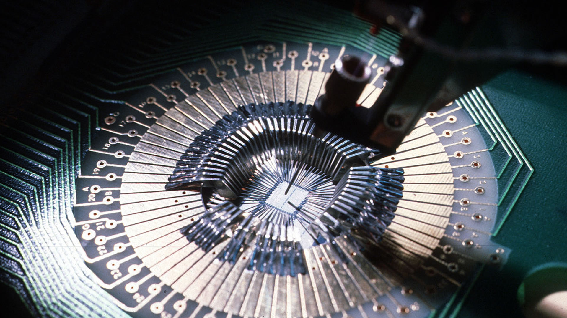
UPDATE: Chinese researchers have just announced a groundbreaking technology that can reduce microchip manufacturing defects by an astounding 99%. This significant advancement could transform the semiconductor industry, ensuring higher quality chips for various applications.
The team, led by Professor Peng Hailin from Peking University, alongside partners from Tsinghua University and HKU, has developed an innovative tool that identifies the sources of flaws during the critical photolithography phase of chip production. This process involves using light to imprint intricate circuit patterns onto silicon wafers, a step that has long been plagued by defects caused by the photoresist material.
Historically, during the development phase, tiny particles from the photoresist can clump together and reattach to the wafer, leading to catastrophic failures in chips, particularly those at 5-nanometer nodes. A mere 30-nanometer particle can render a chip useless, resulting in substantial financial losses for manufacturers.
Until now, manufacturers struggled to visualize these microscopic processes, referring to them as a “black box.” The recent research utilized cryo-electron tomography (cryo-ET), a method typically reserved for biological studies, to freeze the chemical interactions at a frigid 32°F (–175°C). This technique allowed the team to observe the behavior of photoresist polymers in three dimensions, revealing that around 70% of these molecules fail to dissolve correctly, causing defects when rinsed.
The researchers discovered that the tangled polymers form particles through weak hydrophobic interactions, which can lead to chip failures. They proposed two effective solutions that can be integrated into existing manufacturing processes: raising the bake temperature to minimize tangling and altering the rinse procedure to prevent clumps from redepositing on the wafer.
Testing these methods resulted in a dramatic drop in defect counts on 12-inch (30.5 cm) wafers, achieving near-perfect lithography quality. The implications of this breakthrough are immense, potentially revolutionizing the production of semiconductors and safeguarding manufacturers from costly errors.
As the semiconductor industry grapples with increasing demand and the need for improved efficiency, this development marks a pivotal moment. The ability to pinpoint and mitigate defects in microchip production could bolster China’s position in the global tech landscape.
With further developments anticipated, the semiconductor sector is keenly watching how this technology will be adopted and its impact on future chip production standards. This could be a game-changer, not only for Chinese manufacturers but for the entire semiconductor supply chain worldwide.
Stay tuned for more updates on this transformative technology as it unfolds.

Trump Administration Ties Global Health Aid to Abortion Data Sharing

Congress Faces Uncertainty as Trump Questions Health Subsidies

Groundbreaking Research Explores ‘Covert Consciousness’ in Patients

Michael Jordan’s Race Team Takes On NASCAR in Landmark Trial

Chicago Remembers Deadly Our Lady of the Angels Fire, 65 Years Later

Columbus Utility Rates Set to Rise by Up to 18% in 2026

Homemade Ding Dong Cake Recipe Takes Dessert to New Heights
Eurozone Manufacturing PMI Plummets to 49.6, Signals Contraction

Im Si Wan’s New Photos Spark Heated Debate Online

Urgent Update: Tom Aspinall’s Vision Deteriorates After UFC 321

MIT Scientists Uncover Surprising Genomic Loops During Cell Division

University of Hawaiʻi Joins $25.6M AI Project to Enhance Disaster Monitoring

AI Disruption: AWS Faces Threat as Startups Shift Cloud Focus

Time Crystals Revolutionize Quantum Computing Potential

Honeywell Forecasts Record Business Jet Deliveries Over Next Decade

Discover the Full Map of Pokémon Legends: Z-A’s Lumiose City

GOP Faces Backlash as Protests Surge Against Trump Policies

Parenthood Set to Depart Hulu: What Fans Need to Know
-
 Top Stories1 month ago
Urgent Update: Tom Aspinall’s Vision Deteriorates After UFC 321
-
 Health2 months ago
MIT Scientists Uncover Surprising Genomic Loops During Cell Division
-
Science4 weeks ago
University of Hawaiʻi Joins $25.6M AI Project to Enhance Disaster Monitoring
-
 Top Stories1 month ago
AI Disruption: AWS Faces Threat as Startups Shift Cloud Focus
-
 Science2 months ago
Time Crystals Revolutionize Quantum Computing Potential
-
 World2 months ago
Honeywell Forecasts Record Business Jet Deliveries Over Next Decade
-
 Entertainment2 months ago
Discover the Full Map of Pokémon Legends: Z-A’s Lumiose City
-
 Top Stories2 months ago
GOP Faces Backlash as Protests Surge Against Trump Policies
-
 Entertainment2 months ago
Parenthood Set to Depart Hulu: What Fans Need to Know
-

 Politics2 months ago
Judge Signals Dismissal of Chelsea Housing Case Citing AI Flaws
-

 Sports2 months ago
Yoshinobu Yamamoto Shines in Game 2, Leading Dodgers to Victory
-

 Health2 months ago
Maine Insurers Cut Medicare Advantage Plans Amid Cost Pressures